VIPPO in PCB: Meaning, Process, Benefits, and Applications
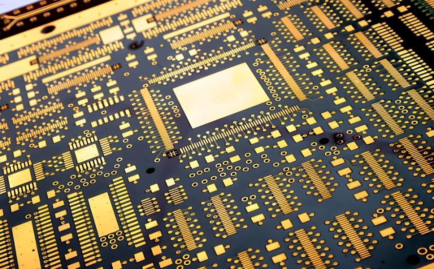
VIPPO in PCB refers to Via-in-Pad Plated Over, a specialized PCB design and manufacturing technique where vias are drilled directly into the component pads and then filled and plated over to create a flat, solderable surface. VIPPO in PCB technology is widely used in high-density, high-performance electronics where space optimization, signal integrity, and thermal management are critical. By placing vias inside the pads, designers can shrink board size, improve routing efficiency, and enhance the overall reliability of the circuit.
Why VIPPO in PCB Matters
VIPPO in PCB is important because it solves several critical challenges found in modern electronics. As devices become more compact, traditional routing methods often create congestion, long trace lengths, and issues related to signal delay. VIPPO allows components to be placed more densely without compromising electrical integrity. The filled and plated-over vias prevent solder wicking and offer a completely flat surface for advanced packages like BGAs, CSPs, and QFNs. This enhances solder joint reliability, reduces void formation, and supports precise component placement during assembly.
How VIPPO in PCB Works
Via Drilling and Formation
The process starts with defining the via structure based on the PCB layout. Microvias or mechanical vias are drilled directly in the pad area of the component. The via depth, diameter, and placement must be optimized for electrical performance and manufacturability.
Via Filling
After drilling, the vias are filled using conductive or non-conductive epoxy. Conductive fill materials help with heat dissipation and electrical performance, while non-conductive fill materials are typically used for high-density, multilayer stack-ups. Proper filling ensures the via barrel is completely sealed, preventing voids and ensuring mechanical strength.
Plating Over
Once filled, the surface is plated with copper to create a smooth, flat pad. This “plated-over” structure is what enables VIPPO to support advanced surface-mounted components. The plating thickness must be controlled carefully to maintain a stable, solderable surface without uneven buildup.
Surface Finish and Assembly
After plating, the board receives a surface finish such as ENIG, ENEPIG, or immersion silver. The finished VIPPO pads allow for accurate soldering during SMT assembly and ensure reliable connections for fine-pitch components.
Advantages of VIPPO in PCB
Improved Signal Integrity
VIPPO in PCB technology shortens trace lengths and minimizes impedance variation. This helps high-frequency signals travel cleanly and reduces issues like crosstalk and electromagnetic interference. Devices such as communication modules, server boards, and RF products depend heavily on this stability.
Better Heat Dissipation
Conductive-filled vias inside the pad help transfer heat away from components more efficiently. This is especially important for processors, power management ICs, and LED drivers where internal temperatures can rise quickly.
Higher Routing Density
VIPPO reduces the need for breakout traces and via dogbones, making it ideal for fine-pitch BGAs and compact multilayer PCBs. By routing through the pad, designers free up more space on inner layers, enabling smaller PCB sizes without compromising performance.
Improved Solder Joint Reliability
Because the filled vias prevent solder from flowing into the hole, VIPPO creates more stable solder joints. This reduces the chances of component tilt, voiding, or early joint failure, especially during lead-free reflow processes that use higher temperatures.
Where VIPPO in PCB Is Used
Smartphones and Wearable Devices
VIPPO is essential for compact PCBs inside smartphones, smartwatches, and wearable trackers. These devices require small form factors and high-performance processors, both of which benefit from VIPPO technology.
High-Density Computing and Servers
Server motherboards, GPUs, and AI accelerator boards use VIPPO to support dense BGA packages with stable signal integrity and excellent thermal performance.
Medical and Aerospace Electronics
Mission-critical electronics in medical imaging devices or aerospace navigation systems rely on VIPPO for durability, electrical precision, and high reliability.
Automotive Electronics
ADAS systems, LED modules, ECUs, and radar units use VIPPO in PCB design to support high-speed signal paths and withstand extreme operating conditions.
Design Considerations for VIPPO in PCB
Pad Size and Via Diameter
Choosing the right via diameter ensures proper filling and plating. A mismatch in pad and via dimensions can lead to solder wicking or poor flatness.
Fill Material Selection
Conductive fill materials improve heat dissipation but cost more. Non-conductive fills suit dense multilayer stack-ups where thermal performance is less critical.
Plating Thickness and Surface Finish
Consistent copper plating is necessary for pad flatness, while finishes like ENIG or ENEPIG offer excellent solderability for fine-pitch components.
Manufacturer Capability
Not all PCB manufacturers can achieve stable, void-free VIPPO structures. Advanced equipment and strict process control are required to produce reliable results.
Conclusion: Build High-Performance Boards With Professional VIPPO Technology
VIPPO in PCB technology is essential for creating high-density, compact, and reliable electronic devices. It enhances signal integrity, improves heat management, and supports advanced components used in modern applications. Whether you are developing smartphones, medical instruments, industrial controls, or next-generation computing products, choosing a capable manufacturing partner is key. For consistent quality, advanced capability, and competitive pricing, you can rely on an experienced VIPPO PCB Manufacturer to bring your design to life with precision and reliability.